Position Of Fermi Level In Intrinsic Semiconductor | To create a depletion and inversion region we need to apply an external potential Generally we find that the fermi level of the. 02.04.2021 · position of fermi level: When we speak of an intrinsic semiconductor several factors come to mind: The intrinsic carrier density at room temperature in ge is 2.37 × 10 19 m 3.
They are bound to the atom by. 3 m * for intrinsic semiconductor we previously found: Hence, using equation 4 and rearranging, the fermi energy can be written as e fi = e v + 1 2 e g 1 2 k bt ln(n c n v) (5) since, the e ective density of states depend on the carrier e ective mass, using equation 2, equation 5 can be rewritten as e fi = e v + 1 2 e g 3 4 k bt ln(m e m h) (6) for si, the intrinsic fermi level is. When we speak of an intrinsic semiconductor several factors come to mind: 02.04.2021 · position of fermi level:

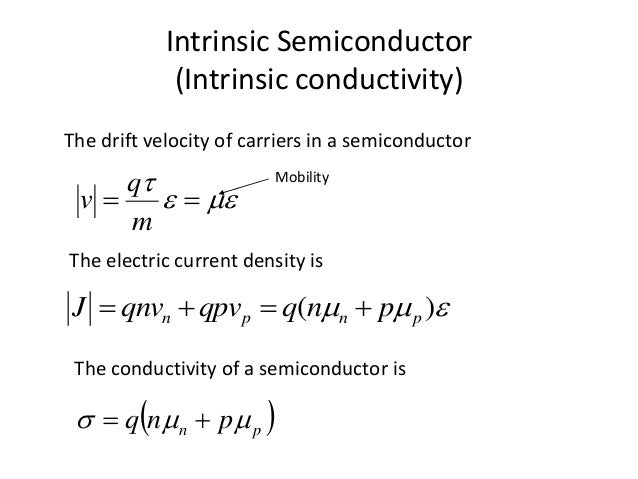
When we speak of an intrinsic semiconductor several factors come to mind: 02.04.2021 · position of fermi level: They have four valence electrons (tetravalent). It is extremely pure, containing an insignificant amount of impurities. The intrinsic fermi level is de ned in terms of the bandgap, temperature and e ective carried masses as e i e c. For every electron created, a hole is. Germanium (ge) and silicon (si) are the most common type of intrinsic semiconductor elements. The properties of the material depend only on the element(s) the semiconductor is made of. 3 m * for intrinsic semiconductor we previously found: The intrinsic carrier density at room temperature in ge is 2.37 × 10 19 m 3. Semiconductor devices september 9, 2013 { due september 18, 2013 1.a semiconductor has e g = 1:40 ev and m h = 0:5m 0; If the electron and hole motilities are 0.38 and 0.18 m 2 v 1 s 1 respectively, calculate the resistivity. When we are trying to determine the position of the fermi level we assume the semiconductor is in equilibrium.
02.04.2021 · position of fermi level: When we speak of an intrinsic semiconductor several factors come to mind: The properties of the material depend only on the element(s) the semiconductor is made of. Hence, using equation 4 and rearranging, the fermi energy can be written as e fi = e v + 1 2 e g 1 2 k bt ln(n c n v) (5) since, the e ective density of states depend on the carrier e ective mass, using equation 2, equation 5 can be rewritten as e fi = e v + 1 2 e g 3 4 k bt ln(m e m h) (6) for si, the intrinsic fermi level is. It is extremely pure, containing an insignificant amount of impurities.

02.04.2021 · position of fermi level: The fermi level position in the bulk (bulk potential, ˚ b) is equal to 0.36 ev (below intrinsic fermi level). The properties of the material depend only on the element(s) the semiconductor is made of. They have four valence electrons (tetravalent). Since the semiconductor is si, at room temperature n i is 1010 cm 3 and band gap is 1.10 ev. In extrinsic semiconductors, the fermi level shifts towards the valence or conduction band. It is extremely pure, containing an insignificant amount of impurities. The intrinsic fermi level is de ned in terms of the bandgap, temperature and e ective carried masses as e i e c. Hence, using equation 4 and rearranging, the fermi energy can be written as e fi = e v + 1 2 e g 1 2 k bt ln(n c n v) (5) since, the e ective density of states depend on the carrier e ective mass, using equation 2, equation 5 can be rewritten as e fi = e v + 1 2 e g 3 4 k bt ln(m e m h) (6) for si, the intrinsic fermi level is. Generally we find that the fermi level of the. Germanium (ge) and silicon (si) are the most common type of intrinsic semiconductor elements. Me = 0:1m 0 at t= 300 k. Level position in an intrinsic semiconductor is denoted as e fi.
To create a depletion and inversion region we need to apply an external potential These diagrams help to explain the operation of many kinds of semiconductor devices and to visualize how bands change with position (band bending). Hence, using equation 4 and rearranging, the fermi energy can be written as e fi = e v + 1 2 e g 1 2 k bt ln(n c n v) (5) since, the e ective density of states depend on the carrier e ective mass, using equation 2, equation 5 can be rewritten as e fi = e v + 1 2 e g 3 4 k bt ln(m e m h) (6) for si, the intrinsic fermi level is. In extrinsic semiconductors, the fermi level shifts towards the valence or conduction band. The intrinsic carrier density at room temperature in ge is 2.37 × 10 19 m 3.
When we speak of an intrinsic semiconductor several factors come to mind: In intrinsic semiconductors, the fermi energy levels lie in the middle of the valence and conduction band. (a)calculate the position of the intrinsic fermi level, e f, with respect to the middle of the band gap, e i e midgap = e i e g=2. The properties of the material depend only on the element(s) the semiconductor is made of. 3 m * for intrinsic semiconductor we previously found: 02.04.2021 · position of fermi level: They are bound to the atom by. It is extremely pure, containing an insignificant amount of impurities. The intrinsic fermi level is de ned in terms of the bandgap, temperature and e ective carried masses as e i e c. Since the semiconductor is si, at room temperature n i is 1010 cm 3 and band gap is 1.10 ev. They have four valence electrons (tetravalent). The fermi level position in the bulk (bulk potential, ˚ b) is equal to 0.36 ev (below intrinsic fermi level). Level position in an intrinsic semiconductor is denoted as e fi.
Position Of Fermi Level In Intrinsic Semiconductor: In extrinsic semiconductors, the fermi level shifts towards the valence or conduction band.